- 您现在的位置:买卖IC网 > Sheet目录2005 > LTC2281IUP#PBF (Linear Technology)IC ADC 10BIT DUAL 64-QFN
LTC2281
9
2281fb
PIN FUNCTIONS
OEA (Pin 58): Channel A Output Enable Pin. Refer to
SHDNA pin function.
SHDNA (Pin 59): Channel A Shutdown Mode Selection
Pin. Connecting SHDNA to GND and OEA to GND results
in normal operation with the outputs enabled. Connecting
SHDNA to GND and OEA to VDD results in normal operation
with the outputs at high impedance. Connecting SHDNA
to VDD and OEA to GND results in nap mode with the
outputs at high impedance. Connecting SHDNA to VDD
and OEA to VDD results in sleep mode with the outputs
at high impedance.
MODE (Pin 60): Output Format and Clock Duty Cycle
Stabilizer Selection Pin. Note that MODE controls both
channels. Connecting MODE to GND selects offset binary
output format and turns the clock duty cycle stabilizer
off. 1/3 VDD selects offset binary output format and turns
the clock duty cycle stabilizer on. 2/3 VDD selects 2’s
complement output format and turns the clock duty cycle
stabilizer on. VDD selects 2’s complement output format
and turns the clock duty cycle stabilizer off.
VCMA (Pin 61): Channel A 1.5V Output and Input Common
Mode Bias. Bypass to ground with 2.2μF ceramic chip
capacitor. Do not connect to VCMB.
SENSEA (Pin 62): Channel A Reference Programming Pin.
Connecting SENSEA to VCMA selects the internal reference
and a ±0.5V input range. VDD selects the internal reference
and a ±1V input range. An external reference greater than
0.5V and less than 1V applied to SENSEA selects an input
range of ±VSENSEA. ±1V is the largest valid input range.
GND (Exposed Pad) (Pin 65): ADC Power Ground. The
Exposed Pad on the bottom of the package needs to be
soldered to ground.
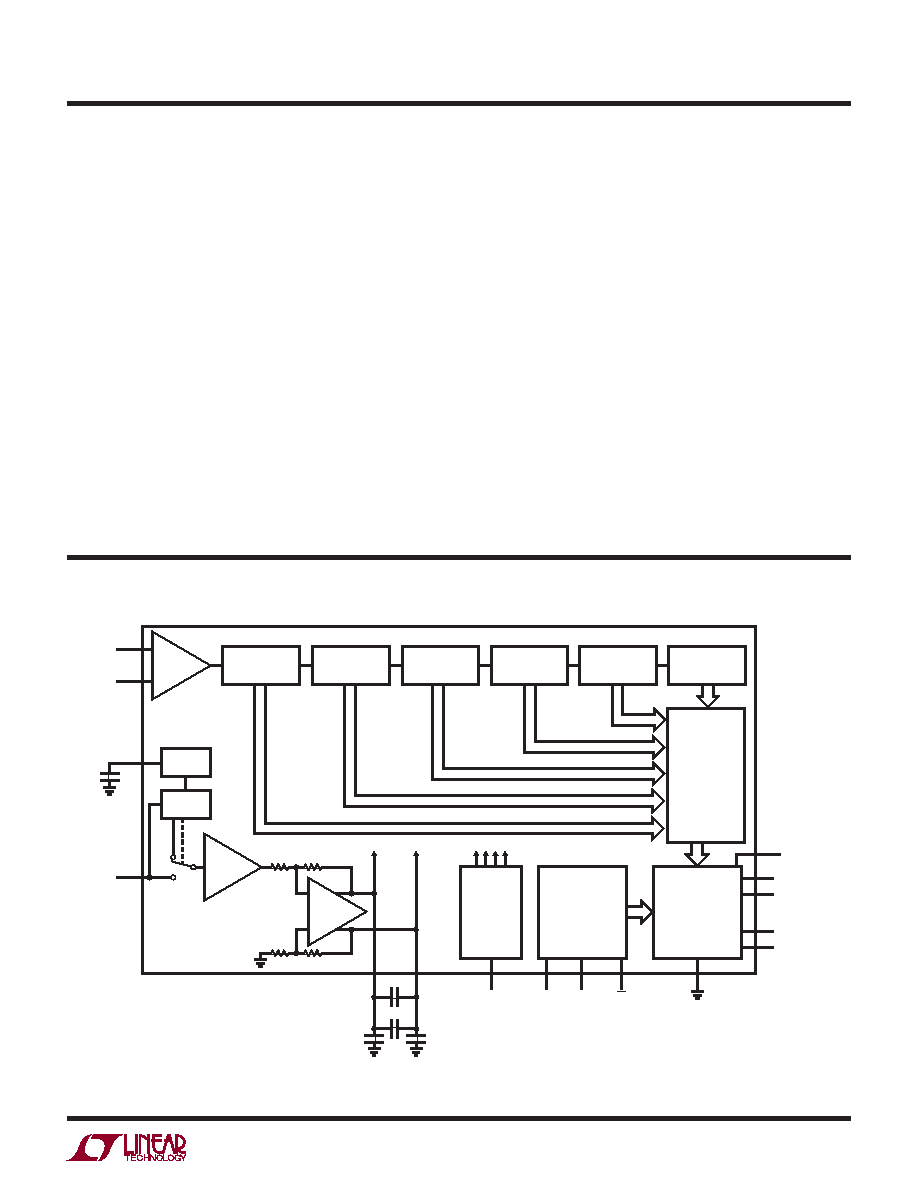
FUNCTIONAL BLOCK DIAGRAM
Figure 1. Functional Block Diagram (Only One Channel is Shown)
SHIFT REGISTER
AND CORRECTION
DIFF
REF
AMP
REF
BUF
2.2μF
1μF
0.1μF
INTERNAL CLOCK SIGNALS
REFH
REFL
CLOCK/DUTY
CYCLE
CONTROL
RANGE
SELECT
1.5V
REFERENCE
FIRST PIPELINED
ADC STAGE
FIFTH PIPELINED
ADC STAGE
SIXTH PIPELINED
ADC STAGE
FOURTH PIPELINED
ADC STAGE
SECOND PIPELINED
ADC STAGE
REFH
REFL
CLK
OE
MODE
OGND
OVDD
2281 F01
INPUT
S/H
SENSE
VCM
AIN
–
AIN
+
2.2μF
THIRD PIPELINED
ADC STAGE
OUTPUT
DRIVERS
CONTROL
LOGIC
SHDN
OF*
D9
D0
CLKOUT*
*OF AND CLKOUT ARE SHARED BETWEEN BOTH CHANNELS.
发布紧急采购,3分钟左右您将得到回复。
相关PDF资料
LTC2282CUP#PBF
IC ADC DUAL 12BIT 105MSPS 64-QFN
LTC2284CUP#PBF
IC ADC DUAL 14BIT 105MSPS 64-QFN
LTC2285CUP#PBF
IC ADC DUAL 14BIT 125MSPS 64QFN
LTC2289IUP#PBF
IC ADC DUAL 10BIT 80MSPS 64QFN
LTC2290IUP#TRPBF
IC ADC DUAL 12BIT 10MSPS 64QFN
LTC2298IUP#PBF
IC ADC DUAL 14BIT 65MSPS 64QFN
LTC2305CDE#TRPBF
IC ADC 12-BIT 2CHN 12-DFN
LTC2306CDD#PBF
IC ADC 12BIT 2CH 500KSPS 10-DFN
相关代理商/技术参数
LTC2281IUP#TRPBF
功能描述:IC ADC DUAL 10BIT 125MSPS 64QFN RoHS:是 类别:集成电路 (IC) >> 数据采集 - 模数转换器 系列:- 标准包装:1 系列:- 位数:14 采样率(每秒):83k 数据接口:串行,并联 转换器数目:1 功率耗散(最大):95mW 电压电源:双 ± 工作温度:0°C ~ 70°C 安装类型:通孔 封装/外壳:28-DIP(0.600",15.24mm) 供应商设备封装:28-PDIP 包装:管件 输入数目和类型:1 个单端,双极
LTC2281IUP-PBF
制造商:LINER 制造商全称:Linear Technology 功能描述:Dual 10-Bit, 125Msps Low Power 3V ADC
LTC2281IUP-TR
制造商:LINER 制造商全称:Linear Technology 功能描述:Dual 10-Bit, 125Msps Low Power 3V ADC
LTC2281IUP-TRPBF
制造商:LINER 制造商全称:Linear Technology 功能描述:Dual 10-Bit, 125Msps Low Power 3V ADC
LTC2281UP
制造商:LINER 制造商全称:Linear Technology 功能描述:Dual 10-Bit, 125Msps Low Power 3V ADC
LTC2282
制造商:LINER 制造商全称:Linear Technology 功能描述:Dual 12-Bit, 105Msps Low Power 3V ADC
LTC2282CUP
制造商:Linear Technology 功能描述:ADC Dual Pipelined 105Msps 12-bit Parallel 64-Pin QFN EP
LTC2282CUP#PBF
功能描述:IC ADC DUAL 12BIT 105MSPS 64-QFN RoHS:是 类别:集成电路 (IC) >> 数据采集 - 模数转换器 系列:- 标准包装:1 系列:- 位数:14 采样率(每秒):83k 数据接口:串行,并联 转换器数目:1 功率耗散(最大):95mW 电压电源:双 ± 工作温度:0°C ~ 70°C 安装类型:通孔 封装/外壳:28-DIP(0.600",15.24mm) 供应商设备封装:28-PDIP 包装:管件 输入数目和类型:1 个单端,双极